

분석 서비스
표면 분석 (성분 분석)
부품의 성분 분석을 위한 최적화된 다양한 분석 서비스를 제공합니다.
▶ 분석 문의/의뢰 : cs@techline.co.kr
Secondary Ion Mass Spectrometry (SIMS)
X-ray Photoelectron Spectroscopy (XPS)/ Electron Spectroscopy of Chemical Analysis
High Resolution X-ray Diffraction (HRXRD)
Field-Emission Auger Electron Microscope (FE-AES)
Scanning Capacitance Microscope (SCM)
Spreading Resistance Probe (SRP)
Fourier Transform-Infrared (FTIR) Spectrometer
Atomic Force Microscope (AFM)
Surface Morphology (α-step)
Thin Film Analyzer
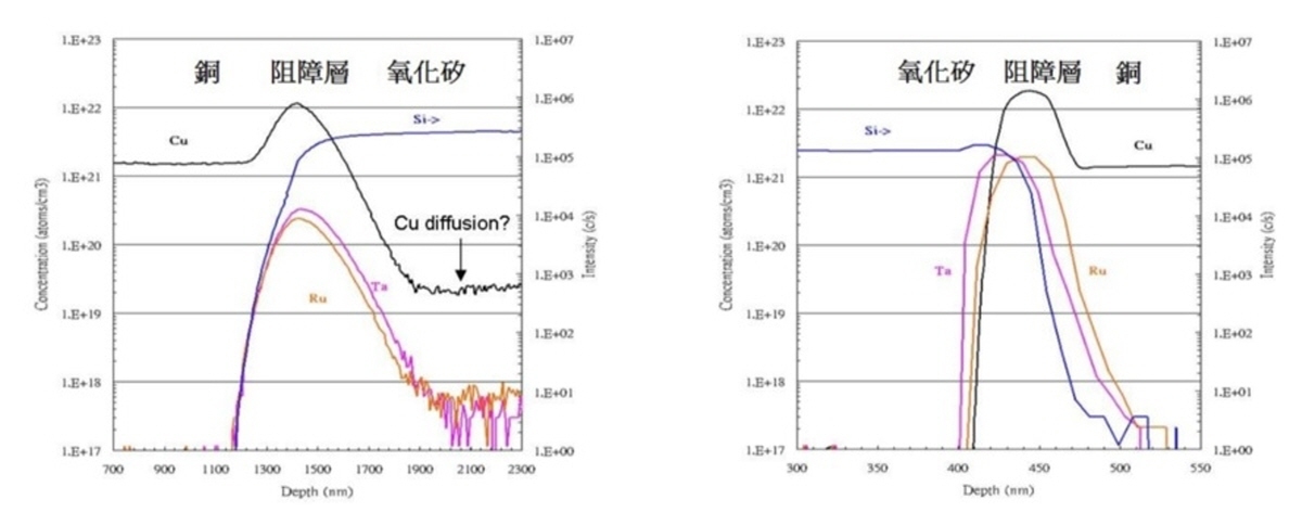
Front side SIMS result : Copper is found in silicon substrate due to an artifact of metal migration caused by incident ion sputtering of SIMS.
Backside SIMS result : Backside SIMS measurement reflects the true result of copper dose and does not diffuse through barrier layer.
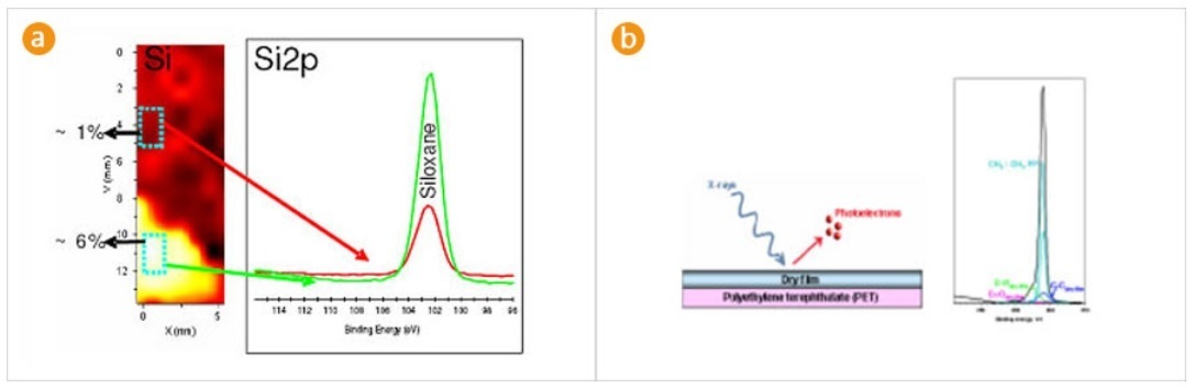
XPS : (a) Adhesion failure issue (b)Identification of photo resist residue
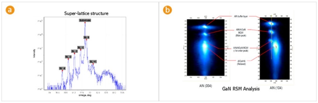
HRXRD : (a) Thickness and composition analysis for a GaN epixaxial film (b) RSM analysis of a GaN epitaxial film
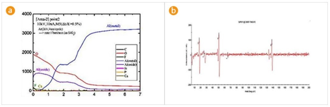
FE-AES : (a) Depth profile of a Al pad (b) AES of a Al pad
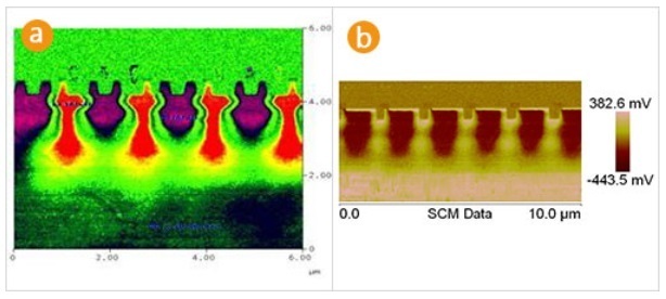
Scanning capacitance microscope : (a) Cross-section dopant distribution on a SRAM sample (b) Dopant distribution on a CIS array
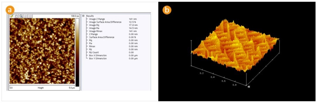
AFM : (a) Surface roughness analysis (b) 3D image
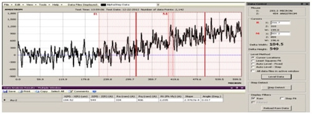
Surface morphology (α-step) : 1D surface roughness analysis
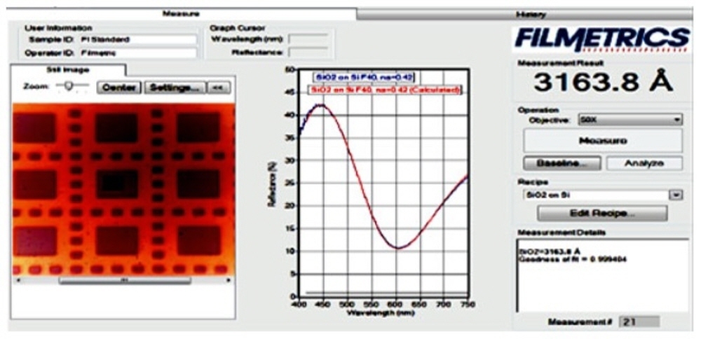
Thin Film Analyzer : Single thin film thickness measurement, SiO2: 316.38 nm