

분석 서비스
재료 분석 (구조 분석)
부품의 구조적 분석을 위한 최적화된 다양한 분석 서비스를 제공합니다.
▶ 분석 문의/의뢰 : cs@techline.co.kr
Focused Ion Beam (FIB)
Transmission Electron Microscope (TEM)
Scanning Electron Microscopy (SEM)
Advanced EELS
Dual Beam Plasma FIB
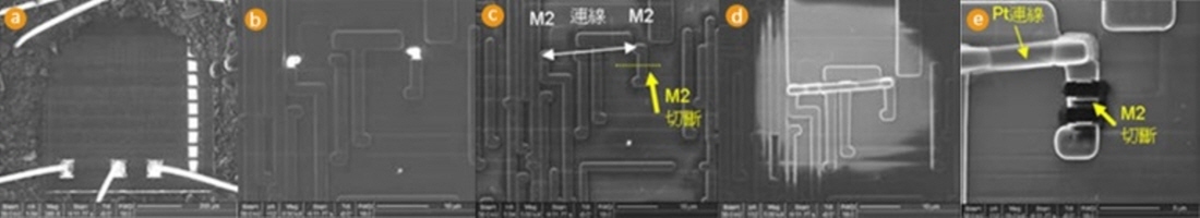
Circuit Editing process. (a) IC decap (b)digging holes and filling metal (c) cutting and connecting wires (d) Deposited pt wire (e) cutting in M2
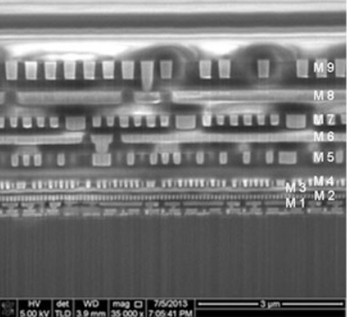
A SEM mode image of a cross-sectional IC
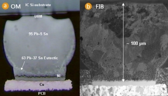
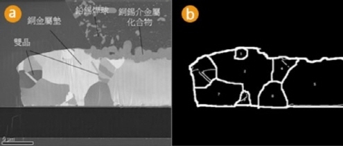
on Channeling Contrast ; Cross-sectional images of a solder ball by (a) OM and (b) FIB
TEM sample preparation : Pre-Thin
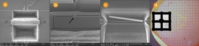
TEM sample preparation : Lift-Out
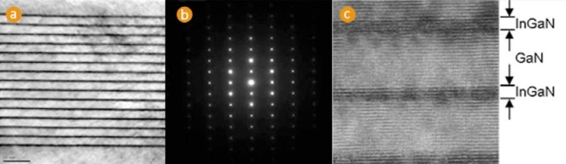
MQW structure of the white LED. (a) Low magnification TEM image. (b) Diffraction pattern (c) High-resolution electron microscope image
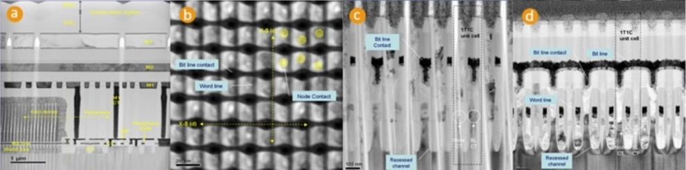
TEM image of Samsung DRAM. (a) Cross-section image (b) The layout of the planar structure (c) Cross-section image along the word line
(d) Cross-section image along the bit line, where recessed gate can be clearly observed.
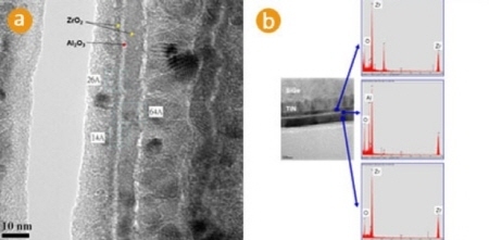
(a) ZrO2 - Al2O3 - ZrO2 dielectric layer in DRAM capacitance (b) ZrO2 - Al2O3 - ZrO2 dielectric layer can be analyzed by TEM/EDX.
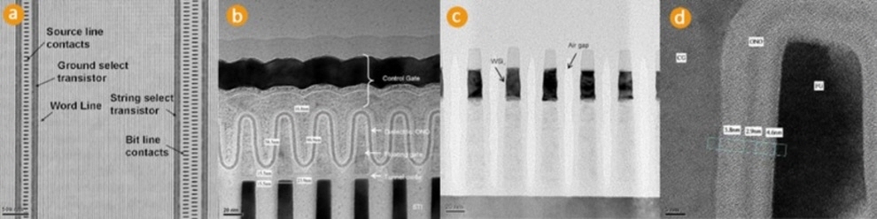
TEM image of Samsung NAND flash. (a) Planar-view image of memory area (b) Cross-section image along word line
(c) Cross-section image along bit line (d) Cross-section image of ONO between FG and CG.
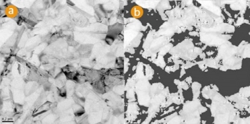
(a) SIM image of Cu grains (b) Locations of Cu grain boundaries after image processing. Twin boundaries have been removed (c) Size distribution of Cu grains.
(a) TEM iamge of poly-Si (b) Locations of poly-Si boundaries after image processing.
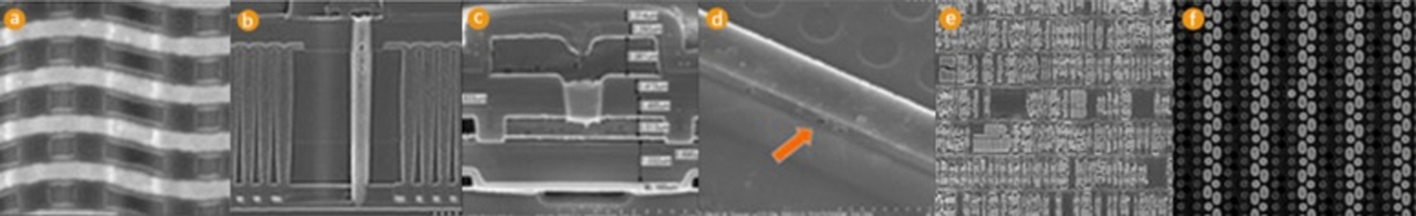
(a)Plan-view observation of DRAM cell after removing capacitors (b) Cross-sectional X-S SEM analysis DRAM cells at word line stitch
(c) Typical X-S SEM observation of IC devices, 2M1P (d) Plan-view SEM observation of ESD failure
(e) IC reverse engineering (f) Passive Voltage Contrast (PVC)
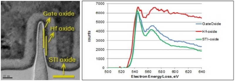
Near edge fine structures of EELS was used to analyze chemical state of the oxygen in different materials of the 16nm high-k materials
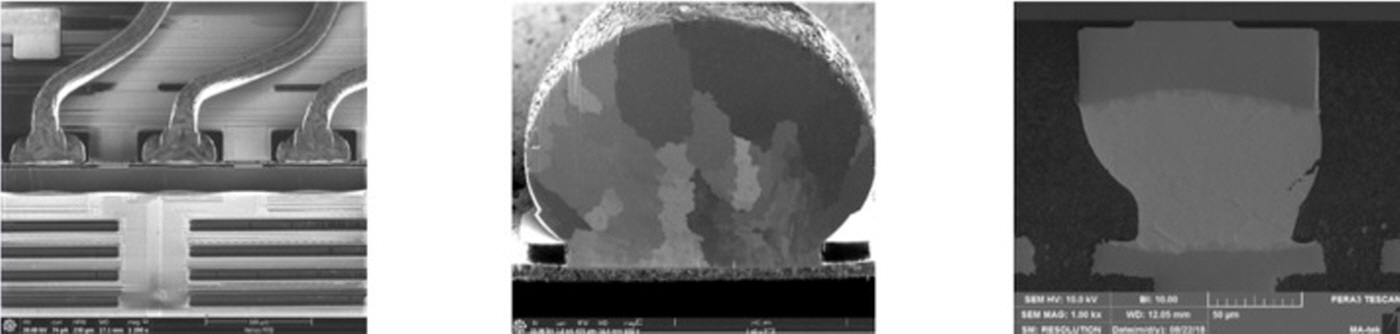
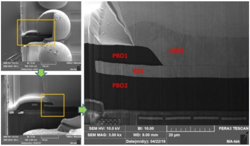
Bond pad and wire inspection, Solder bump inspection by channel contrast, C4 bump cross-section
Profile checking under BGA ball in CSP
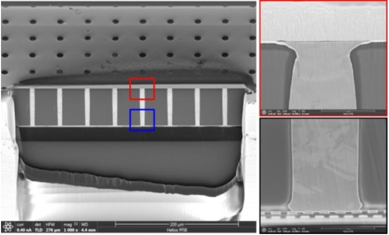
TSV inspection