

분석 서비스
불량 분석
반도체 및 부품의 고장분석은 제품 개발 및 양산 시 발생하는 고장의 원인 파악 및 개선에 필수 요소로서, 다양한 고장 분석 방법을 통해 최적의 분석 솔루션을 제공합니다.
▶ 분석 문의/의뢰 : cs@techline.co.kr
Destructive Analysis (파괴 분석)
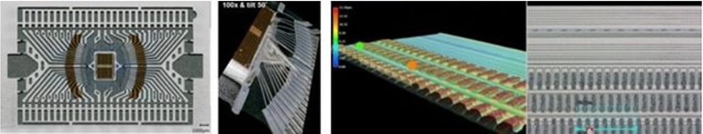
Decap and Delayer by Chemical
Decap and Delayer by Laser
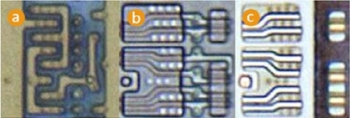
Decap and Delayer by Parallel Lapping
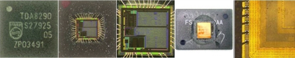
Chemical Decap and Laser Decap
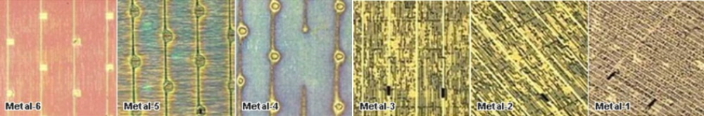
OM Image after Delayer
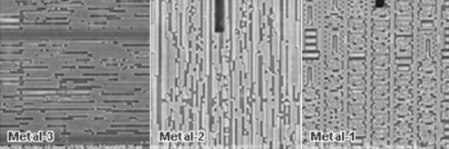
SEM Image after Delayer
Non-Destructive Analysis (비파괴 분석)
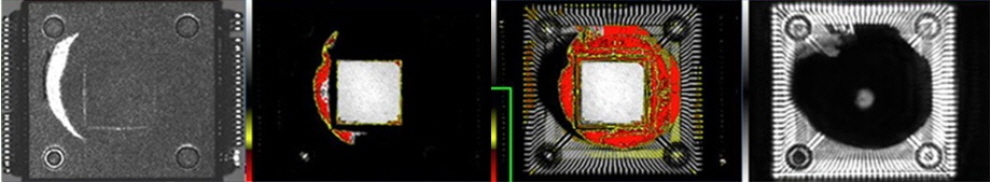
X-Ray
Scanning Acoustic Through (SAT)
Optical Profiler (OP)
3D X-Ray Microscopy
High-Resolution 3D Optical Microscopy
Time Domain Reflectometry (TDR)
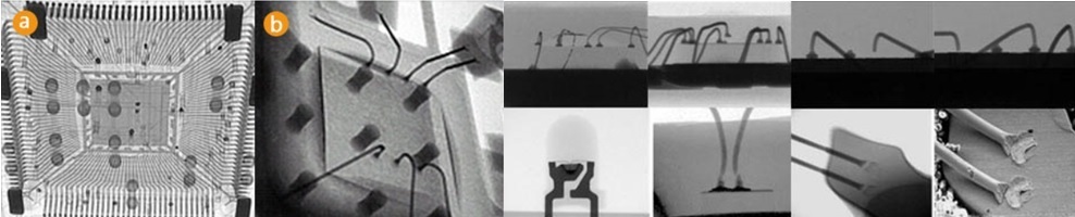
X-Ray (2D and Tilt)
Optical microscopy (OM)
SAT Anylysis
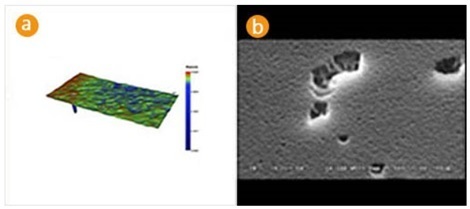
Optical profiler (OP)
3D X-ray microscopy ; Cu Wire
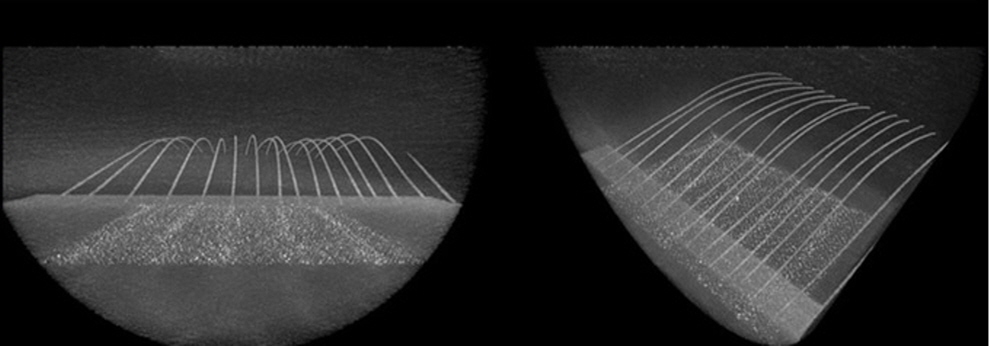
3D X-ray microscopy ; Al Wire
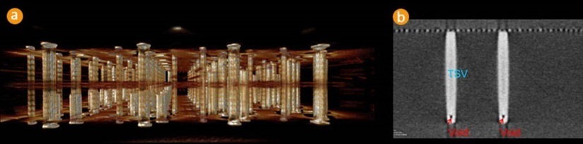
3D X-ray microscopy ; (a)PCB substrat (b) TSV void
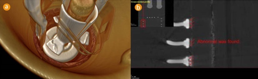
3D X-ray microscopy ; (a)Mini motor (b) Wire lifting
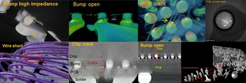
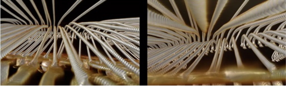
High-resolution 3D optical microscopy ; Wire Bonding and Gold Bump
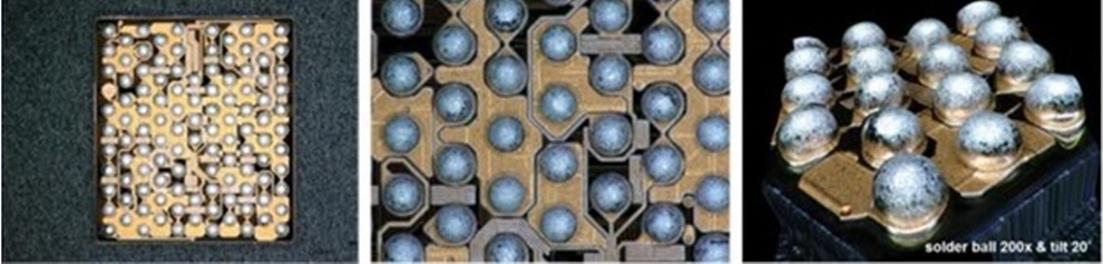
High-resolution 3D optical microscopy ; WLCSP
Electrical Analysis (전기적 분석)
- Emission Microscopy (EMMI)
- InGaAs
- Optical Beam Induced Resistance Change (OBIRCH)
- Conductive Atomic Force Microscopy & Electric Field Microscopy
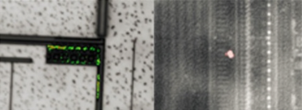
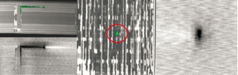
- Thermal Emission Microscopy
- Nano Probing
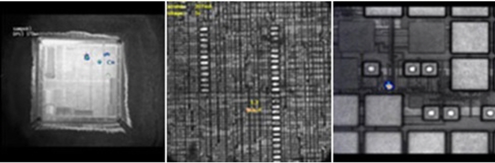
Emission microscopy (EMMI)
InGaAs
Optical Beam Induced Resistance Change (OBIRCH)
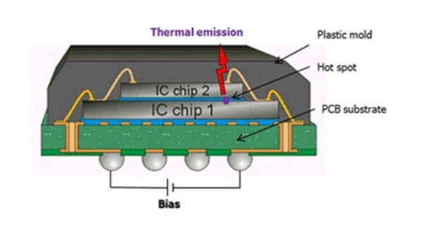
Thermal emission analysis image through IC’s front side